Description:
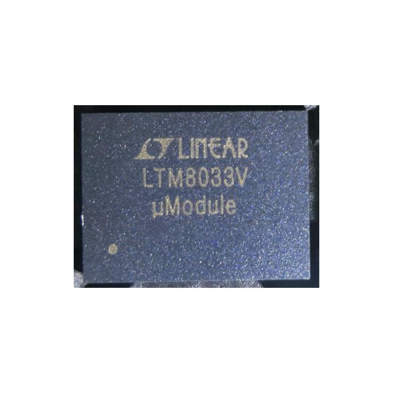
The LTM8033IV#PBF is an electromagnetic compatible (EMC) 36V, 3A DC/DC μModule® (power module) buck converter designed to meet the radiated emissions requirements of EN55022. Conducted emission requirements can be met by adding standard filter components. Included in the package are the switching controller, power switches, inductor, filters and all support components. Operating over an input voltage range of 3.6V to 36V, the LTM8033 supports an output voltage range of 0.8V to 24V, and a switching frequency range of 200kHz to 2.4MHz, each set by a single resistor. Only the bulk input and output filter capacitors are needed to finish the design.
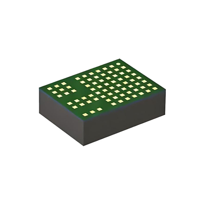
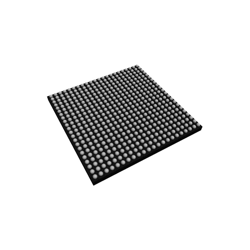
The LTM8033IV#PBF is packaged in a compact (11.25mm × 15mm × 4.32mm) overmolded land grid array (LGA) and ball grid array (BGA) package suitable for automated assembly by standard surface mount equipment. The LTM8033 is available with SnPb (BGA) or RoHS compliant terminal finish.
Features:
Complete Step-Down Switch Mode Power Supply
Wide Input Voltage Range: 3.6V to 36V
3A Output Current
0.8V to 24V Output Voltage
EN55022 Class B Compliant
Current Share Multiple LTM8033 Regulators for More Than 3A Output
Selectable Switching Frequency: 200kHz to 2.4MHz
Current Mode Control
SnPb or RoHS Compliant Finish
Programmable Soft-Start
Compact Package (11.25mm × 15mm × 4.32mm)
Surface Mount LGA and (11.25mm × 15mm × 4.92mm) BGA Packages
Applications:
Automotive Battery Regulation
Power for Portable Products
Distributed Supply Regulation
Industrial Supplies
Wall Transformer Regulation
PIN FUNCTIONS
VOUT (Bank 1): Power Output Pins. Apply the output filter capacitor and the output load between these pins and GND pins.
GND (A8, Bank 2): Tie these GND pins to a local ground plane below the LTM8033 and the circuit components. Return the feedback divider (RADJ) to this net.
FIN (Bank 3): Filtered Input. This is the node after the input EMI filter. Apply the capacitor recommended by Table 1. Additional capacitance may be applied if there is a need to modify the behavior of the integrated EMI filter; otherwise, leave these pins unconnected. See the Applications Information section for more details.
VIN (Bank 4): The VIN pin supplies current to the LTM8033’s internal regulator and to the internal power switch. This pin must be locally bypassed with an external, low ESR capacitor; see Table 1 for recommended values. Ensure that VIN + BIAS is less than 56V.
SHARE (Pin A6): Tie this to the SHARE pin of another LTM8033 when paralleling the outputs. Otherwise, do not connect.
ADJ (Pin A7): The LTM8033 regulates its ADJ pin to 0.79V. Connect the adjust resistor from this pin to ground. The value of RADJ is given by the equation RADJ = 394.21/(VOUT – 0.79), where RADJ is in kΩ.
RT (Pin B6): The RT pin is used to program the switching frequency of the LTM8033 by connecting a resistor from this pin to ground. The Applications Information section of the data sheet includes a table to determine the resistance value based on the desired switching frequency. Minimize capacitance at this pin.
SYNC (Pin B8): This is the external clock synchronization input. Ground this pin for low ripple Burst Mode® operation at low output loads. Tie to a stable voltage source greater than 0.7V to disable Burst Mode operation. Do not leave this pin floating. Tie to a clock source for synchronization. Clock edges should have rise and fall times faster than 1μs. See the Synchronization section in the Applications Information section.
PGOOD (Pin B7): The PGOOD pin is the open-collector output of an internal comparator. PGOOD remains low until the ADJ pin is greater than 90% of the final regulation voltage. PGOOD output is valid when VIN is above 3.6V and RUN/SS is high. If this function is not used, leave this pin floating.
AUX (Pin G3): Low Current Voltage Source for BIAS. In many designs, the BIAS pin is simply connected to VOUT. The AUX pin is internally connected to VOUT and is placed adjacent to the BIAS pin to ease printed circuit board routing. Although this pin is internally connected to VOUT, it is not intended to deliver a high current, so do not connect this pin to the load. If this pin is not tied to BIAS, leave it floating.
BIAS (Pin G4): The BIAS pin connects to the internal power bus. Connect to a power source greater than 2.8V and less than 25V. If the output is greater than 2.8V, connect this pin there. If the output voltage is less, connect this to a voltage source between 2.8V and 25V but ensure that VIN + BIAS is less than 56V.
RUN/SS (Pin G8): Pull the RUN/SS pin below 0.2V to shut down the LTM8033. Tie to 2.5V or more for normal operation. If the shutdown feature is not used, tie this pin to the VIN pin. RUN/SS also provides a soft-start function; see the Applications Information section.

