Description:
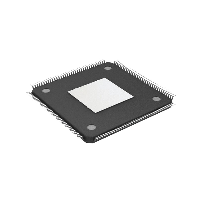
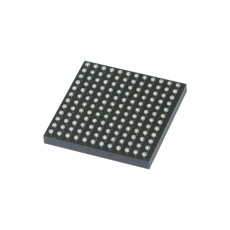
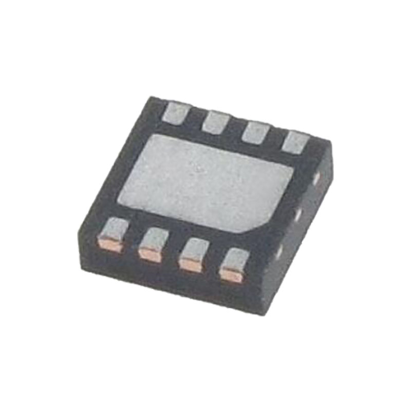
The ESD5481 is designed to protect voltage sensitive components from ESD. Excellent clamping capability, low leakage and fast response time provide best in class protection on designs that are exposed to ESD. Because of its small size, it is suited for use in cellular phones, MP3 players, digital cameras and many other portable applications where board space comes at a premium.
Features:
·Low Capacitance 15 pF
· Low Clamping Voltage
· Small Body Outline Dimensions: 0.60 mm x 0.30 mm
· Low Body Height: 0.3 mm
· Stand−off Voltage: 5.0 V
· Low Leakage
· Response Time is < 1 ns
· IEC61000−4−2 Level 4 ESD Protection
· IEC61000−4−4 Level 4 EFT Protection
· These Devices are Pb−Free, Halogen Free/BFR Free and are RoHS Compliant
Mechanical Characteristics
MOUNTING POSITION: Any
QUALIFIED MAX REFLOW TEMPERATURE: 260°C
Device Meets MSL 1 Requirements
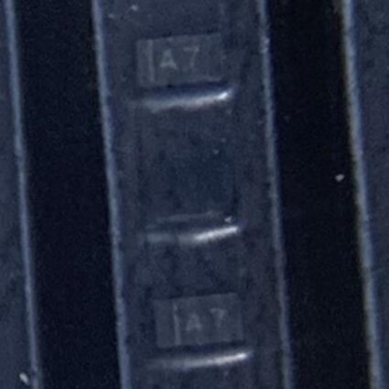
MARKING DIAGRAM :AM
Applications:
Suitable for cellular phones, MP3 players, digital cameras, and many other portable applications where board space is extremely valuable.
ELECTRICAL CHARACTERISTICS
(TA = 25°C unless otherwise noted)
| Symbol | Parameter |
| IPP | Maximum Reverse Peak Pulse Current |
| VC | Clamping Voltage @ IPP |
| VRWM | Working Peak Reverse Voltage |
| IR | Maximum Reverse Leakage Current @ VRWM |
| VBR | Breakdown Voltage @ IT |
| IT | Test Current |
| RDYN | Dynamic Resistance |
*See Application Note AND8308/D for detailed explanations of datasheet parameters.
ANSI/ESD STM5.5.1 − Electrostatic Discharge Sensitivity Testing using Transmission Line Pulse (TLP) Model. TLP conditions: Z0 = 50 , tp = 100 ns, tr = 4 ns, averaging window; t1 = 30 ns to t2 = 60 ns.
ESD Voltage Clamping
For sensitive circuit elements it is important to limit the voltage that an IC will be exposed to during an ESD event to as low a voltage as possible. The ESD clamping voltage is the voltage drop across the ESD protection diode during an ESD event per the IEC61000−4−2 waveform. Since the IEC61000−4−2 was written as a pass/fail spec for larger systems such as cell phones or laptop computers it is not clearly defined in the spec how to specify a clamping voltage at the device level. onsemi has developed a way to examine the entire voltage waveform across the ESD protection diode over the time domain of an ESD pulse in the form of an oscilloscope screenshot, which can be found on the datasheets for all ESD protection diodes. For more information on how onsemi creates these screenshots and how to interpret them please refer to AND8307/D.
NOTE: TLP parameter: Z0 = 50 , tp = 100 ns, tr = 300 ps, averaging window: t1 = 30 ns to t2 = 60 ns. VIEC is the equivalent voltage stress level calculated at the secondary peak of the IEC 61000−4−2 waveform at t = 30 ns with 2 A/kV. See TLP description below for more information.
Transmission Line Pulse (TLP) Measurement
Transmission Line Pulse (TLP) provides current versus voltage (I−V) curves in which each data point is obtained from a 100 ns long rectangular pulse from a charged transmission line. A simplified schematic of a typical TLP system is shown in Figure 7. TLP I−V curves of ESD protection devices accurately demonstrate the product’s ESD capability because the 10s of amps current levels and under 100 ns time scale match those of an ESD event. This is illustrated in Figure 8 where an 8 kV IEC 61000−4−2 current waveform is compared with TLP current pulses at 8 A and 16 A. A TLP I−V curve shows the voltage at which the device turns on as well as how well the device clamps voltage over a range of current levels. For more information on TLP measurements and how to interpret them please refer to AND9007/D.


