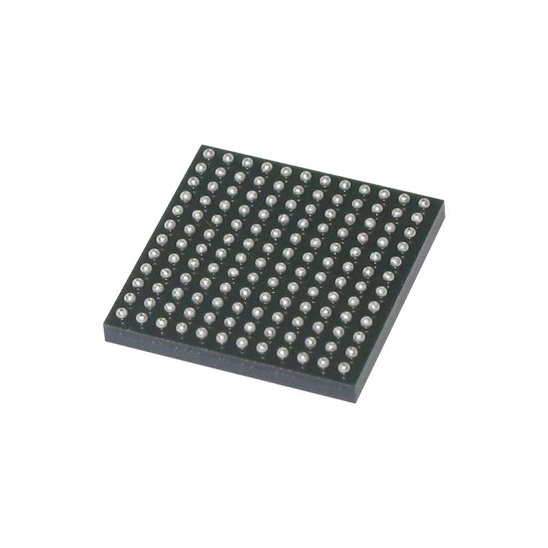
Description:
The CY7C027 and CY7C028 are low power CMOS 32K, 64K × 16 dual-port static RAMs. Various arbitration schemes are included on the devices to handle situations when multiple processors access the same piece of data. Two ports are provided, permitting independent, asynchronous access for reads and writes to any location in memory. The devices can be used as standalone 16-bit dual-port static RAMs or multiple devices can be combined to function as a 32-bit or wider master/slave dual-port static RAM. An M/S pin is provided for implementing 32-bit or wider memory applications without the need for separate master and slave devices or additional discrete logic. Application areas include interprocessor and multiprocessor designs, communications status buffering, and dual-port video/graphics memory.
Each port has independent control pins: dual chip enables (CE0 and CE1), read or write enable (R/W), and output enable (OE). Two flags are provided on each port (BUSY and INT). BUSY signals that the port is trying to access the same location currently being accessed by the other port. The interrupt flag (INT) permits communication between ports or systems by means of a mail box. The semaphores are used to pass a flag, or token, from one port to the other to indicate that a shared resource is in use. The semaphore logic is comprised of eight shared latches. Only one side can control the latch (semaphore) at any time. Control of a semaphore indicates that a shared resource is in use. An automatic power down feature is controlled independently on each port by the chip enable pins
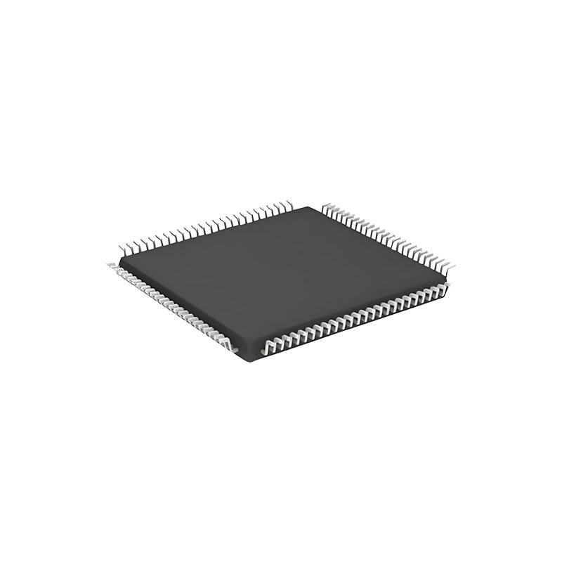
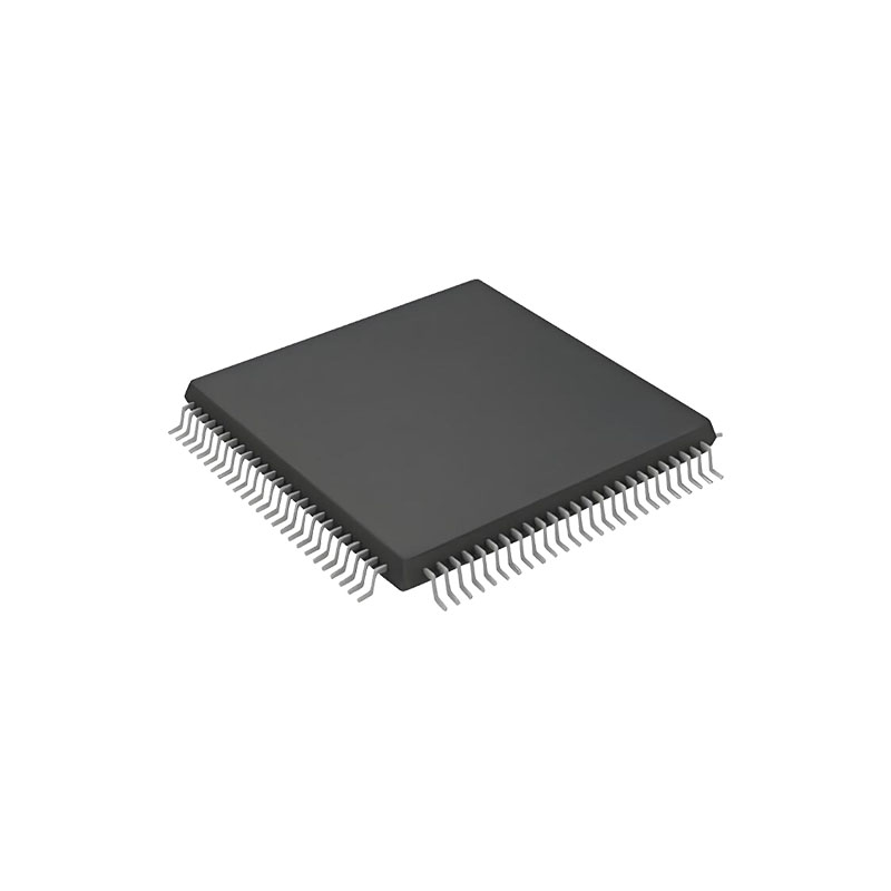
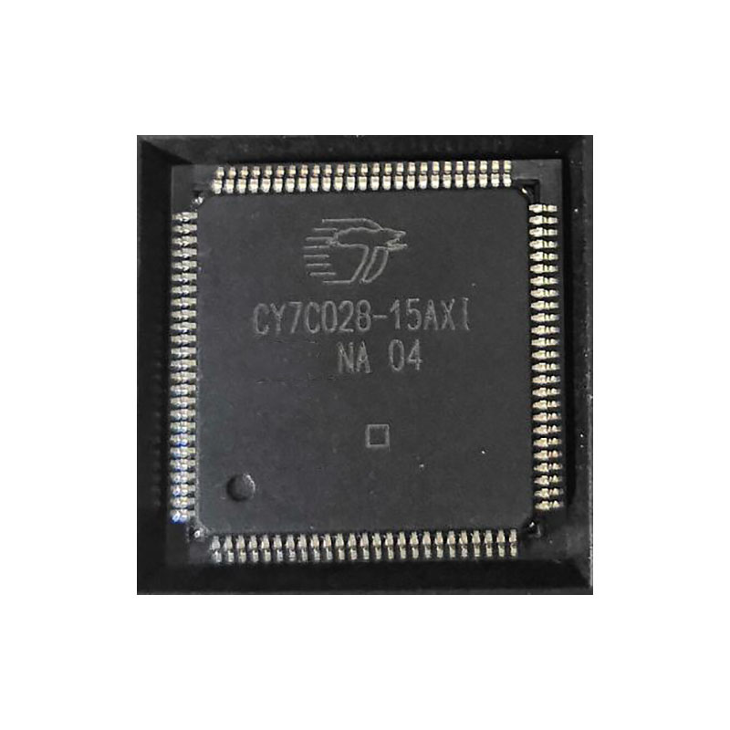
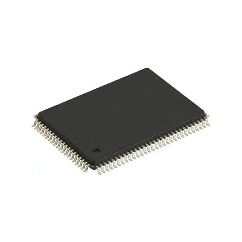
The CY7C027 and CY7C028 are available in 100-pin Thin Quad Flat pack (TQFP) packages.
The CY7C027 and CY7C028 are Obsolete
Features:
True dual-ported memory cells which allow simultaneous access of the same memory location
64K × 16 organization (CY7C028)
0.35 micron CMOS for optimum speed and power
High speed access: 15 and 20 ns
Low operating power
Active: ICC = 180 mA (typical)
Standby: ISB3 = 0.05 mA (typical)
Fully asynchronous operation
Automatic power down
Expandable data bus to 32 bits or more using Master/Slave chip select when using more than one device
On-chip arbitration logic
Semaphores included to permit software handshaking between ports
INT flags for port-to-port communication
Separate upper-byte and lower-byte control
Dual chip enables
Pin select for Master or Slave
Commercial and industrial temperature ranges
Available in 100-pin TQFP
Pb-free packages available
Data Retention Mode:
The CY7C027 and CY7C028 are designed with battery backup in mind. Data retention voltage and supply current are guaranteed over temperature. The following rules ensure data retention:
- Chip enable (CE) must be held HIGH during data retention, within VCC to VCC – 0.2 V.
- CE must be kept between VCC – 0.2 V and 70% of VCC during the power up and power down transitions.
- The RAM can begin operation > tRC after VCC reaches the minimum operating voltage (4.5 V).
NOTES:
Tested initially and after any design or process changes that may affect these parameters
CE = VCC, VIN = GND to VCC, TA = 25 °C. This parameter is guaranteed but not tested.
Architecture:
The CY7C027 and CY7C028 consist of an array of 32K and 64K words of 16 bits each of dual-port RAM cells, I/O and address lines, and control signals (CE, OE, R/W). These control pins permit independent access for reads or writes to any location in memory. To handle simultaneous writes/reads to the same location, a BUSY pin is provided on each port. Two interrupt (INT) pins can be used for port-to-port communication. Two semaphore (SEM) control pins are used for allocating shared resources. With the M/S pin, the devices can function as a master (BUSY pins are outputs) or as a slave (BUSY pins are inputs). The devices also have an automatic power down feature controlled by CE. Each port is provided with its own output enable control (OE), which allows data to be read from the device.

