Description:
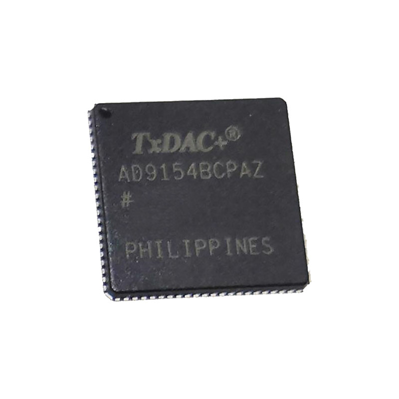
AD9154BCPAZ is a four channel, 16 bit, high dynamic range analog-to-digital converter that can generate multiple carriers up to Nyquist frequency in baseband mode, providing a maximum sampling rate of 2.4 GSPS. This product has optimization functions for product output, power detection of input signals (such as complex digital modulation), gain, phase and offset compensation, and direct conversion transmission applications., It can be directly docked with ADI’s ADRF6720-27 RF orthogonal modulator. In mixed mode, the product can reconstruct the carrier in the second and third Nyquist regions. The serial port interface allows for programming and reading back internal parameters. Can be programmed within the full scale output current range of 4 mA to 20 mA.
Ultrawide signal bandwidth enables emerging wideband and multiband wireless applications.
Advanced low spurious and distortion design techniques provide high quality synthesis of wideband signals from baseband to high intermediate frequencies.
JESD204B Subclass 1 support simplifies multichip synchronization.
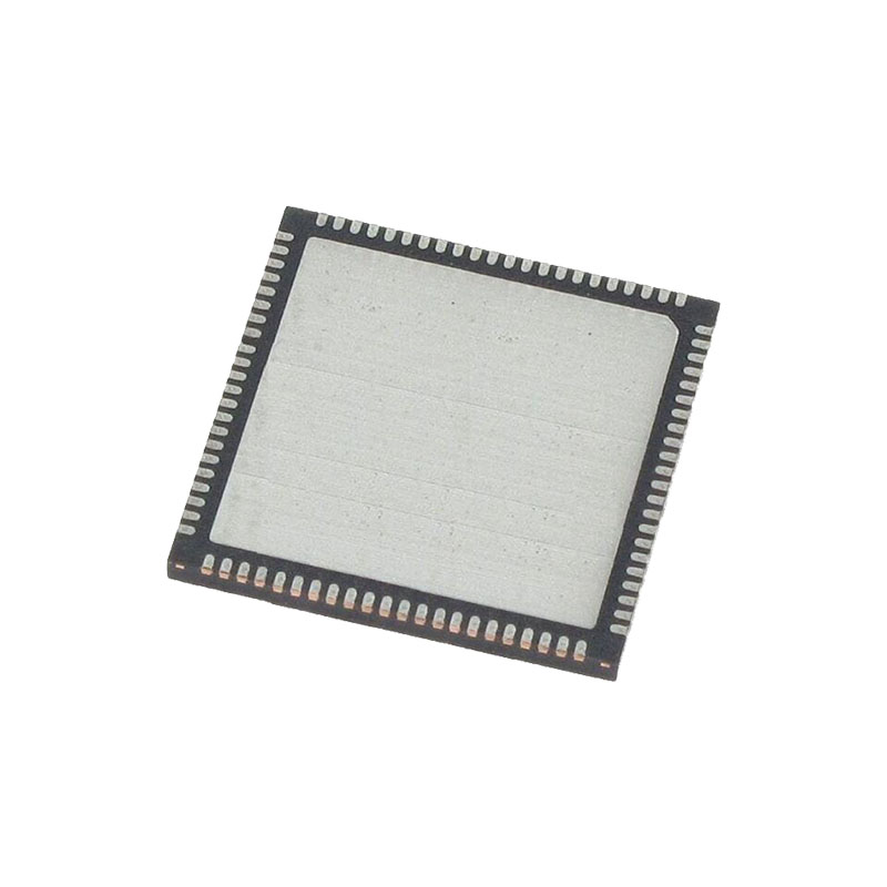
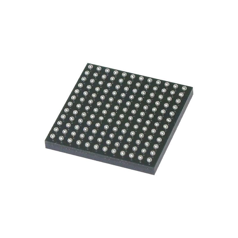
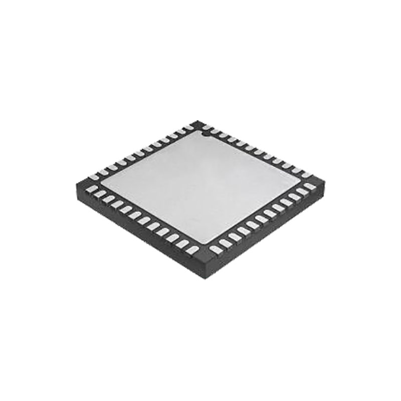
Small package size with a 12 mm × 12 mm footprint.
Features:
Input speed can reach up to 1 GSPS
Exclusive, low spurious and distorted design
Single carrier parameters: LTE 20 MHz bandwidth (BW), ACLR=77 dBc,180 MHz IF
Six carrier parameters: GSM IMD=78 dBc, with a download wave interval of 600 kHz at 180 MHz IF
SFDR=72 dBc, 180 MHz IF, − 6 dBFS single tone
Equipped with 8-lane JESD204B interface
Support multi chip synchronization
Fixed delay
Data generator delay compensation
Can perform input signal power detection
High performance, low noise phase-locked loop (PLL) clock multiplier
Digital anti sine filter
Digital orthogonal modulation using digital controlled oscillators
Nyquist frequency band hybrid mode
Optional interpolation filters for 1, 2, 4, and 8
Low power parameters: 2.11 W, 1.6 GSPS
Full operating conditions
Applications:
Wireless communications,Wideband repeaters,Point to point microwave radio,Software defined radios,Instrumentation,Transmit diversity, multiple input/multiple output (MIMO)
SERIAL PORT OPERATION
The serial port interface (SPI) is a flexible, synchronous serial communications port that allows easy interfacing with many industry-standard microcontrollers and microprocessors. The interface facilitates read/write access to all registers that configure the AD9154. MSB first or LSB first transfer formats are supported.
The SPI is configurable as a 4-wire interface or a 3-wire interface in which the input and output share a single-pin I/O, SDIO.
There are two phases to a communication cycle with the AD9154. Phase 1 is the instruction cycle (the writing of an instruction byte into the device), coincident with the first 16 SCLK rising edges. The instruction word provides the serial port controller with information regarding the data transfer cycle, Phase 2 of the communication cycle. The Phase 1 instruction word defines whether the upcoming data transfer is a read or write, along with the starting register address for the following data transfer.
A logic high on the CS pin, followed by a logic low, resets the serial port timing to the initial state of the instruction cycle.
From this state, the next 16 rising SCLK edges represent the instruction bits of the current input/output (I/O) operation.
The remaining SCLK edges are for Phase 2 of the communication cycle. Phase 2 is the actual data transfer between the device and the system controller. Phase 2 of the communication cycle is a transfer of one or more data bytes. Eight × N SCLK cycles are needed to transfer N bytes during the transfer cycle. Registers change immediately upon writing to the last bit of each transfer byte, except for the frequency tuning word (FTW) and numerically controlled oscillator (NCO) phase offsets, which change only when the frequency tuning word FTW_UPDATE_REQ bit is set.
DATA FORMAT
R/W, Bit 15 of the instruction word, determines whether a read or a write data transfer occurs after the instruction word write. Logic 1 indicates a read operation, and Logic 0 indicates a write operation. A14 to A0, Bit 14 to Bit 0 of the instruction word, determine the register accessed during the data transfer portion of the communication cycle. For multibyte transfers, A[14:0] is the starting address. The device generates the remaining register addresses based on the address increment bits. If the address increment bits are set high (Register 0x000, Bit 5 and Bit 2), multibyte SPI writes start on A[14:0] and increment by 1 every eight bits sent/ received. If the address increment bits are set to 0, the address decrements by 1 every eight bits

