Description:
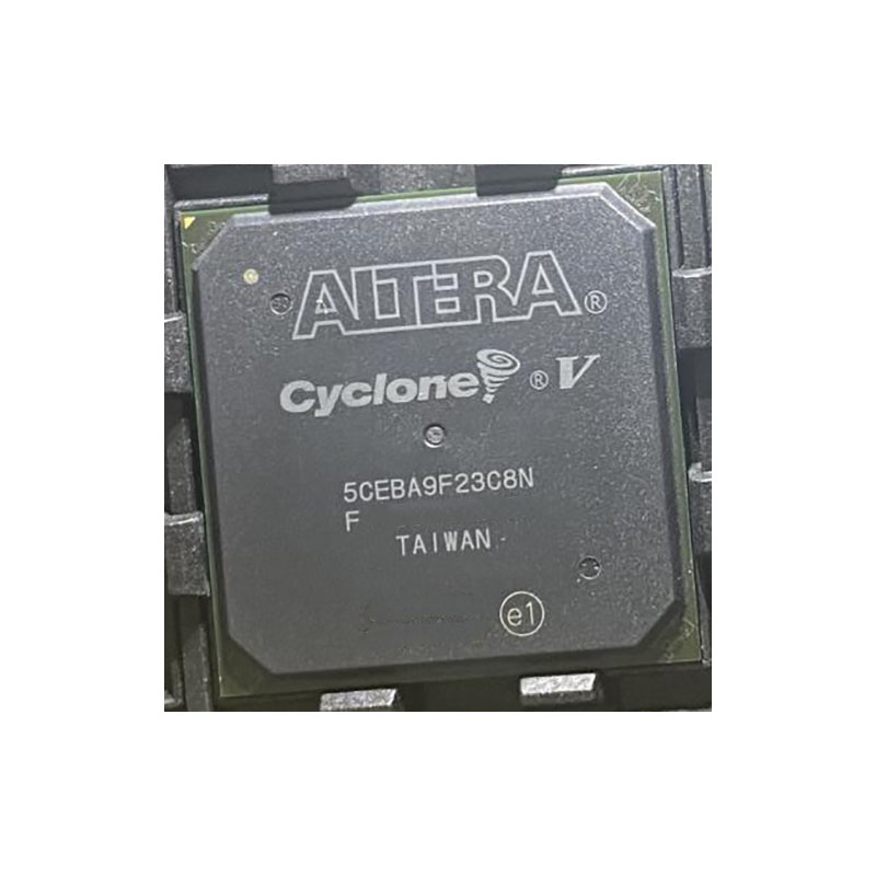
The Cyclone® V devices are designed to simultaneously accommodate the shrinking power consumption, cost, and time-to-market requirements; and the increasing bandwidth requirements for high-volume and cost-sensitive applications.
Cyclone V E are optimized for the lowest system cost and power requirement for a wide spectrum of general logic and DSP applications.
Key Advantages of Cyclone® V Devices
Lower power consumption
Built on TSMC’s 28 nm low-power (28LP) process technology and includes an abundance of hard intellectual property (IP) blocksUp to 40% lower power consumption than the previous generation device
Improved logic integration and differentiation capabilities
8-input adaptive logic module (ALM)
Up to 13.59 megabits (Mb) of embedded memory
Variable-precision digital signal processing (DSP) blocks
Increased bandwidth capacity
- gabitsper second (Gbps) and 144 Gbpstransceivers
- Hard memory controllers
Hard processor system (HPS) with integrated Arm* Cortex* -A9 MPCore* processor
Tight integration of a dual-core Arm* Cortex* -A9 MPCore* processor, hard IP, and an FPGA in a single Cyclone® V system-on-a-chip (SoC)
Supports over 128 Gbps peak bandwidth with integrated data coherency between the processor and the FPGA fabric
Lowest system cost
Requires only two core voltages to operate
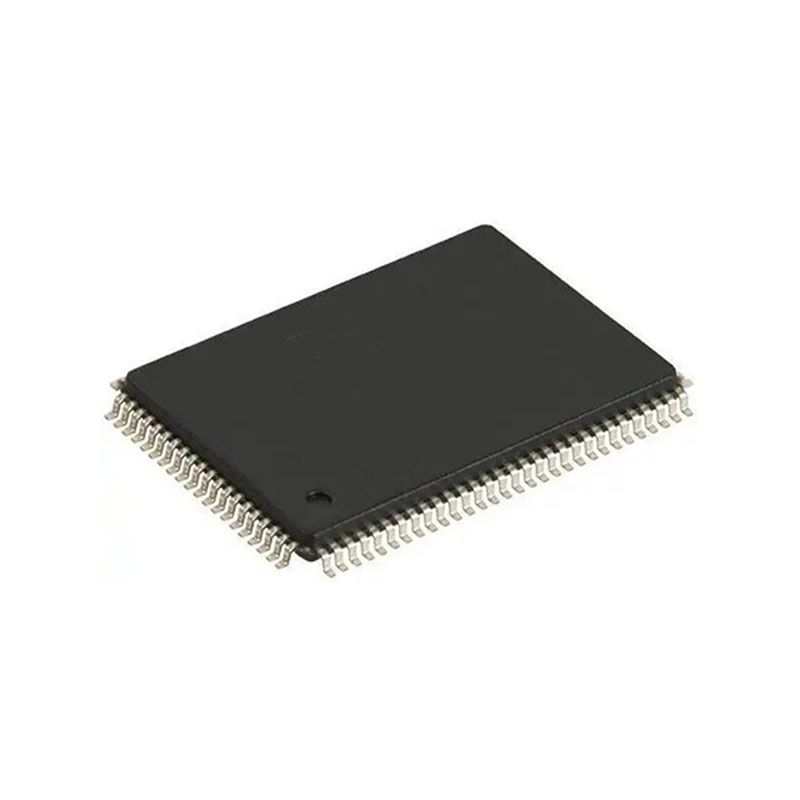
Available in low-cost wirebond packaging
Includes innovative features such as Configuration via Protocol (CvP) and partial reconfiguration
Features
Technology
- TSMC’s 28-nm low-power (28LP) process technology
- 1.1 V core voltage
Packaging
- Wirebond low-halogen packages
- Multiple device densities with compatible package footprints for seamless migration between different device densities
- RoHS-compliant and leaded(1)options
High-performance FPGA fabric Enhanced 8-input ALM with four registers
Internal memory blocks
- M10K—10-kilobits (Kb) memory blocks with soft error correction code (ECC)
- Memory logic array block (MLAB)—640-bit distributed LUTRAM where you can use up to 25% of the ALMs as MLAB memory
Embedded Hard IP blocks
Variable-precision DSP
- Native support for up to three signal processing precision levels (three 9 x 9, two 18 x 18, or one 27 x 27 multiplier) in the same variable-precision DSP block
- 64-bit accumulator and cascade
- Embedded internal coefficient memory
- Preadder/subtractor for improved efficiency
Memory controller DDR3, DDR2, and LPDDR2 with 16 and 32 bit ECC support
Embedded transceiver I/O PCI Express* (PCIe*) Gen2 and Gen1 (x1, x2, or x4) hard IP with multifunction support, endpoint, and root port
Clock networks
- Up to 550 MHz global clock network
- Global, quadrant, and peripheral clock networks
- Clock networks that are not used can be powered down to reduce dynamic power
Phase-locked loops (PLLs)
- Precision clock synthesis, clock delay compensation, and zero delay buffering (ZDB)
- Integer mode and fractional mode
FPGA General-purpose I/Os (GPIOs)
- 875 megabits per second (Mbps) LVDS receiver and 840 Mbps LVDS transmitter
- 400 MHz/800 Mbps external memory interface
- On-chip termination (OCT)
- 3.3 V support with up to 16 mA drive strength
Low-power high-speed serial interface
- 614 Mbps to 6.144 Gbps integrated transceiver speed
- Transmit pre-emphasis and receiver equalization
- Dynamic partial reconfiguration of individual channels
HPS (Cyclone V SE, SX, and ST devices only)
- Single or dual-core Arm Cortex-A9 MPCore processor-up to 925 MHz maximum frequency with support for symmetric and asymmetric multiprocessing
- Interface peripherals—10/100/1000 Ethernet media access control (EMAC), USB 2.0 On-The-GO (OTG) controller, quad serial peripheral interface (QSPI) flash controller, NAND flash controller, Secure Digital/MultiMediaCard (SD/MMC) controller, UART, controller area network (CAN), serial peripheral interface (SPI), I2C interface, and up to 85 HPS GPIO
interfaces
- System peripherals—general-purpose timers, watchdog timers, direct memory access (DMA) controller, FPGA configuration manager, and clock and reset managers
- On-chip RAM and boot ROM
- HPS–FPGA bridges—include the FPGA-to-HPS, HPS-to-FPGA, and lightweight HPS-to-FPGA bridges that allow the FPGA fabric to issue transactions to slaves in the HPS, and vice versa
- FPGA-to-HPS SDRAM controller subsystem—provides a configurable interface to the multiport front end (MPFE) of the HPS SDRAM controller
- Arm CoreSight™ JTAG debug access port, trace port, and on-chip trace storage
Configuration
- Tamper protection—comprehensive design protection to protect your valuable IP investments
- Enhanced advanced encryption standard (AES) design security features
- CvP
- Dynamic reconfiguration of the FPGA
- Active serial (AS) x1 and x4, passive serial (PS), JTAG, and fast passive parallel (FPP) x8 and x16 configuration options
- Internal scrubbing
- Partial reconfiguration
Applications:
Enhanced with integrated transceivers and hard memory controllers, the Cyclone® V devices are suitable for applications in the industrial, wireless and wireline, military, and automotive markets.

