Description:
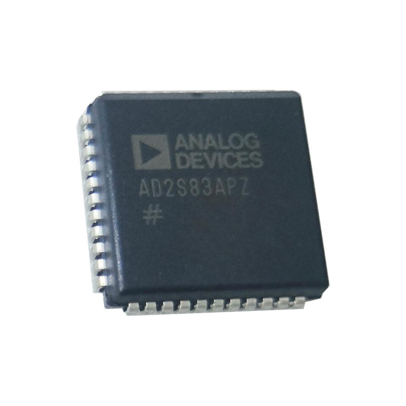
The AD2S83APZ is a monolithic 10-, 12-, 14-, or 16-bit tracking resolver-to-digital converter.
The converter allows users to select their own resolution and dynamic performance with external components. The converter allows users to select the resolution to be 10, 12, 14, or 16 bits and to track resolver signals rotating at up to 1040 revs per second (62,400 rpm) when set to 10-bit resolution.
The AD2S83APZ converts resolver format input signals into a parallel natural binary digital word using a ratiometric tracking conversion method. This ensures high noise immunity and tolerance of long leads allowing the converter to be located remote from the resolver.
A precise analog signal proportional to velocity is also available and will replace a tachogenerator. The AD2S83 operates over reference frequencies in the range 0 Hz to 20,000 Hz.
Features:
Tracking R/D Converter
High Accuracy Velocity Output
High Max Tracking Rate 1040 RPS (10 Bits)
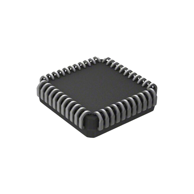
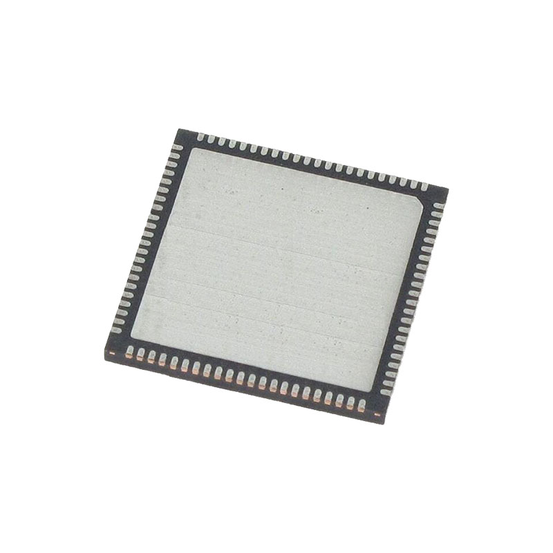
44-Lead PLCC Package
10-, 12-, 14-, or 16-Bit Resolution Set by User
Ratiometric Conversion
Stabilized Velocity Reference
Dynamic Performance Set by User
Industrial Temperature Range
APPLICATIONS
DC and AC Servo Motor Control
Process Control
Numerical Control of Machine Tools
Robotics
Axis Control
PRODUCT HIGHLIGHTS
High Accuracy Velocity Output. A precision analog velocity signal with a typical linearity of ±0.1% and reversion error less than ±0.3% is generated by the AD2S83. The provision of this signal removes the need for mechanical tachogenerators used in servo systems to provide loop stabilization and speed control.
Resolution Set by User. Two control pins are used to select the resolution of the AD2S83 to be 10, 12, 14 or 16 bits allowing optimum resolution for each application. Ratiometric Tracking Conversion. This technique provides continuous output position data without conversion delay. It also provides noise immunity and tolerance of harmonic distortion on the reference and input signals.
Dynamic Performance Set by the User. By selecting external resistor and capacitor values the user can determine bandwidth, maximum tracking rate and velocity scaling of the converter to match the system requirements. The component values are easy to select using the free component selection software design aid.
CONNECTING THE CONVERTER
The power supply voltages connected to +VS and –VS pins should be +12 V dc and –12 V dc and must not be reversed. The voltage applied to VL can be +5 V dc to +VS. It is recommended that the decoupling capacitors are connected in parallel between the power lines +VS, –VS and ANALOG GROUND adjacent to the converter. Recommended values are 100 nF (ceramic) and 10 µF (tantalum). Also capacitors of 100 nF and 10 µF should be connected between +VL and DIGITAL GROUND adjacent to the converter. When more than one converter is used on a card, separate decoupling capacitors should be used for each converter.
The resolver connections should be made to the SIN and COS inputs, REFERENCE INPUT and SIGNAL GROUND as shown in Figure 11 and described in the Connecting the Resolver section.
The two signal ground wires from the resolver should be joined at the SIGNAL GROUND pin of the converter to minimize the coupling between the sine and cosine signals. For this reason it is also recommended that the resolver is connected using individually screened twisted pair cables with the sine, cosine and reference signals twisted separately.
SIGNAL GROUND and ANALOG GROUND are connected internally. ANALOG GROUND and DIGITAL GROUND must be connected externally and as close to the converter as possible.
CONVERTER RESOLUTION
Two major areas of the AD2S83 specification can be selected by the user to optimize the total system performance. The resolution of the digital output is set by the logic state of the inputs SC1 and SC2 to be 10, 12, 14 or 16 bits; and the dynamic characteristics of bandwidth and tracking rate are selected by the choice of external components.
The choice of the resolution will affect the values of R4 and R6 which scale the inputs to the integrator and the VCO respectively (see Component Selection section). If the resolution is changed, then new values of R4 and R6 must be switched into the circuit.
Note: When changing resolution under dynamic conditions, do it when the BUSY is low, i.e., when data is not changing.
