Description:
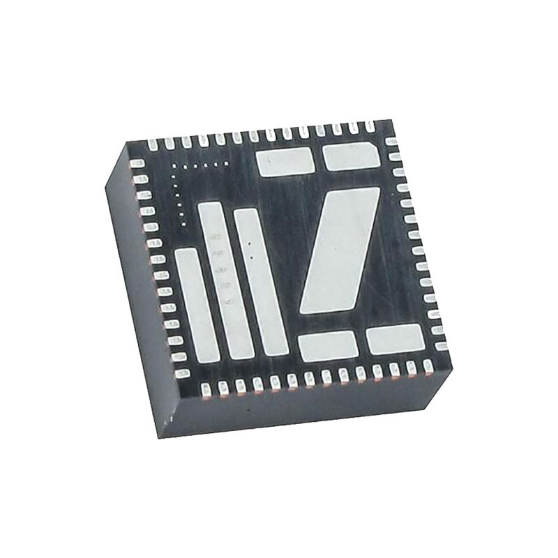
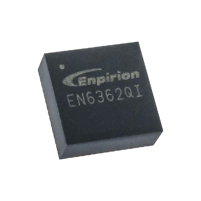
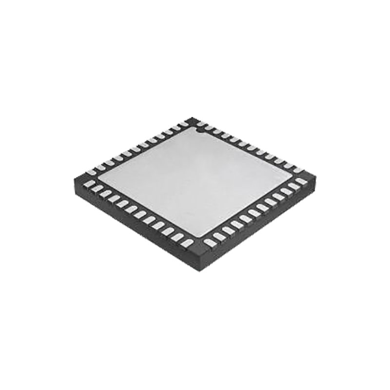
The EN6362QI is a Power System on a Chip (PowerSoC) DC to DC converter with an integrated inductor, PWM controller, MOSFETs and compensation to provide the smallest solution size in an 8x8x3mm 56 pin QFN module.
It offers very high efficiency and is able to provide 6A continuous output current with no de-rating. The EN6362QI also provides excellent line and load regulation over temperature. The EN6362QI is specifically designed to meet the precise voltage and fast transient requirements of high-performance, low-power processor, DSP, FPGA, memory boards and system level applications in distributed power architecture.
Other features include precision enable threshold, prebias monotonic start-up, and programmable soft start.
The device’s advanced circuit techniques, ultra-high switching frequency, and proprietary integrated inductor technology deliver high-quality, ultra-compact DC-DC conversion.
The Altera Enpirion integrated inductor solution significantly helps to reduce noise. The complete power converter solution enhances productivity by offering greatly simplified board design, layout and manufacturing requirements.
Features:
High Efficiency (Up to 96%)
Excellent Ripple and EMI Performance
Up to 6A Continuous Operating Current
Input Voltage Range (3.0V to 6.5V)
1.5% VFB Accuracy
Optimized Total Solution Size (160 mm2)
Precision Enable Threshold for Sequencing
Programmable Soft-Start
Pin compatible with the 8A EN6382QI
Thermal, Over-Current, Short Circuit, Reverse Current Limit and Under-Voltage Protections
RoHS Compliant, MSL Level 3, 260°C Reflow
Applications:
Point of load regulation for FPGAs, ASICs, processors, DSPs, and distributed power
architectures.
Industrial automation, servers, storage, adapter cards, wireless base stations, test and measurement, and embedded computing.
Space constrained applications that require the highest power density.
Noise sensitive applications.
Functional Description
The EN6362QI is a synchronous buck power supply with integrated power MOSFET switches and integrated inductor. The switching supply uses voltage mode control and a low noise PWM topology. The nominal input voltage range is 3.0 – 6.5 volts. The output voltage is programmed using an external resistor divider network. The feedback control loop incorporates a type IV voltage mode control design. Type IV voltage mode control maximizes control loop bandwidth and maintains excellent phase margin to improve transient performance. Although the EN6362QI is guaranteed to support up to 6A continuous output current operation over the full ambient temperature range (thermal design), the peak current supported before reaching OCP is substantially higher, exceeding 10A. The operating switching frequency can be adjusted by an external resistor between 0.7MHz and 1.7MHz. The high switching frequency enables the use of small-size input and output capacitors.
EN6362QI electrical features at a glance:
• Precision Enable Threshold
• Soft-Start
• Pre-bias Start-Up
• Resistor Programmable Switching Frequency
• Power Good
• Over-Current/Short Circuit Protection
• Reverse Current Limit (RCL)
• Thermal Shutdown (OTP) with Hysteresis
• Under-Voltage Lockout
Precision Enable;
The ENABLE threshold is a precision analog voltage rather than a digital logic threshold. A precision voltage reference and a comparator circuit are kept powered up even when ENABLE is de-asserted. The narrow voltage gap between ENABLE Logic Low and ENABLE Logic High (about 100mV hysteresis) allows the device to turn on at a precise enable voltage level. The precise enable threshold, in conjunction with the proper choice of soft-start capacitors allows accurate sequencing for multiple power supplies. ENABLE has a 2ms lockout time that prevents the device from re-enabling immediately after it has been disabled.
Soft-Start
The SS pin, in conjunction with a small external capacitor between this pin and AGND provides the soft-start function, designed to limit in-rush current during start-up. When the part is enabled, soft-start (SS) current generator charges the SS capacitor in a linear manner. As long as the SS voltage level is smaller than the feedback reference (about 0.6V) the SS voltage is used as feedback reference, ensuring a linear increase of the output voltage. Once the voltage on the SS capacitor reaches 0.6V, the minimum detector (Figure 20) will select the bandgap reference as target, while the voltage across the SS capacitor will continue ramping up until it reaches about 1.5V. As the SS voltage slew rate depends on the SS capacitor, so does the output voltage. The rise time is defined as the time needed by the output voltage to go from zero to 95% of the programmed value. The rise time (tRISE) is given by the following equation: tRISE [ms] = Css [nF] x 0.065 There are no limitations regarding the value of the SS capacitor, but the usual range is between 10nF and 100nF.
Resistor Programmable Frequency
The operation of the EN6362QI can be optimized by a proper choice of the RFQADJ resistor. If high efficiency is the most important factor, then a lower switching frequency should be selected, while if a better transient response is the most important factor, a higher switching frequency should be selected.
